

COMPLEX TESTS
Solutions for Semiconductor Testing
Enabling Post-silicon Validation and Test
Our semiconductor test portfolio is built on three pillars
- Validation and Test Engineering Services
- Test systems design and development
- Application-specific products and solutions
Whether you’re validating complex mixed-signal ICs and SoCs, specific IPs, or advanced sensor and RF modules, our services and solutions will help reduce validation time, improve test coverage, and ensure long-term product quality.
Mixed-Signal
Power Management
Memories
RF Devices
WLR & Parametric
Validation and Test Engineering Services
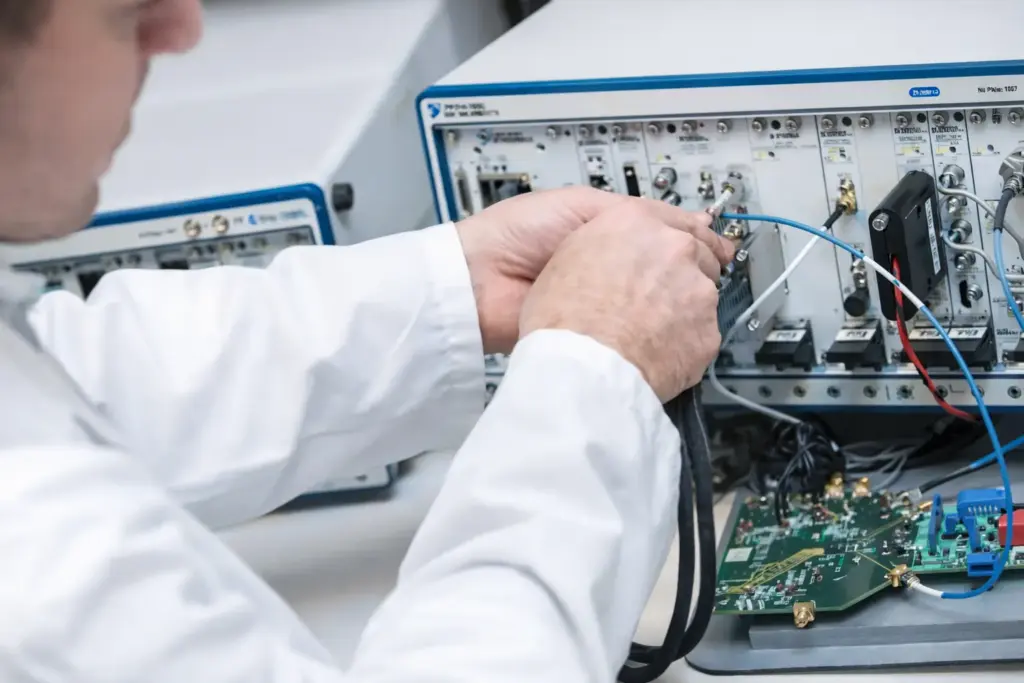
Semiconductor validation and test campaigns are often constrained by time, limited engineering resources, and growing system complexity. Recruiting and onboarding engineers with deep domain expertise and hands-on lab experience can be time-consuming – especially during critical project phases.
NOFFZ Technologies provides validation and test engineering services that seamlessly augment your teams with experienced semiconductor test engineers. Our engineers integrate efficiently into your workflows, tools, and processes to accelerate execution while maintaining full transparency and technical ownership on your side.
We don’t just run tests – we help define what to test, how to test it, and how to interpret the results. By working closely with design and project teams, we reduce iteration cycles, improve result quality, and enable confident engineering decisions throughout the validation process.
Our Services
Test Strategy & Plan Development
- Definition of structured validation and test plans aligned with device architecture, operating conditions, and key performance targets.
Custom Test Hardware Development
- Design and development of load boards, interface boards, and custom connection solutions to ensure reliable DUT access and accurate measurements.
Test Program Development, Execution & DUT Debug
- Development and execution of automated test programs, including data analysis and root-cause investigation to accelerate issue resolution.
Reporting & Design Feedback
- Preparation of structured test reports and data summaries that provide clear, actionable feedback to design and project teams.
Our Value
Engineering-Driven Partnership
- Our engineers combine in-depth expertise in semiconductor test platforms (NI PXI, NI STS, V93K) and software environments (C#, LabVIEW, Python, C++)
Flexible Deployment Models
- We support customers globally through a mix of on-site collaboration and remote execution, enabling fast ramp-up and scalable project support.
High Value at Competitive Cost
- Our delivery model allows us to provide high-quality engineering services at a competitive cost, helping customers optimize project budgets without compromising technical depth or execution quality.
Test systems design and development
Semiconductor test systems must be designed around the specific requirements of the device, the test strategy, and the target phase of the product lifecycle.
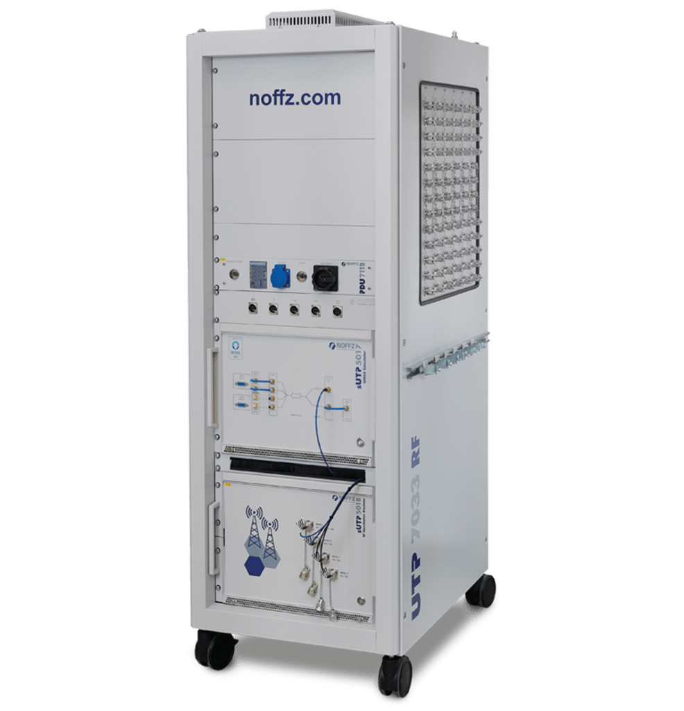
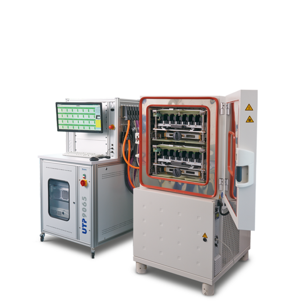
NOFFZ Technologies brings extensive experience in the architecture, design, and development of semiconductor test systems for both validation and production test. We design complete test solutions that integrate test instrumentation, interfaces, software, and automation – aligned with device characteristics and project objectives.
- Validation Test Systems – optimized for measurement accuracy, flexibility, and evolving test requirements, enabling deep insight into device behavior throughout the development cycle.
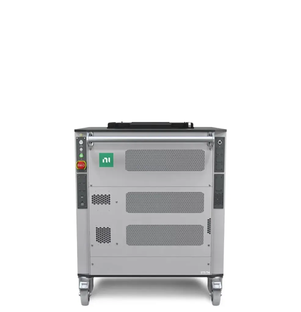
- Production Test Systems – built for high-volume semiconductor manufacturing, with a strong focus on robustness, throughput, and cost of test. Depending on project requirements, production solutions can be fully custom-designed test systems or systems based on the NI STS platform, leveraging its scalability and production-proven architecture.
NOFFZ UTP 7033
NOFFZ UTP 9065
NI-STS (Semiconductor Test System) platform
Application-Specific Products and Solutions
FLT 150A
FLT 150A
PMIC Fast Load Transient
Fast load transients represent one of the most critical stress conditions for modern power management ICs and voltage regulators. Rapid current steps can expose stability issues, control loop weaknesses, and transient response limitations that are not visible in static or slow dynamic tests.
Our FLT 150A is a dedicated test instrument designed to generate high-current, high-slew-rate load transients with deterministic and repeatable behavior. It delivers programmable dynamic current profiles with slew rates up to 150A/µs, enabling accurate reproduction of fast load steps, pulse trains, and complex transient sequences. Its FPGA-based control architecture ensures nanosecond-level timing determinism, allowing engineers to correlate load events precisely with voltage response and measurement instrumentation.
Key Features:
- High-bandwidth current control with real-world transient emulation up to 150A/µs and 200 ns pulse timing resolution
- Accurate, time-aligned measurements using a 20 MHz Rogowski coil, precision Hall sensor, and 50 MS/s voltage and current acquisition
- Flexible synchronization and triggering with external load start and trigger outputs to align other instruments to the exact transient event
- Seamless system integration via LabVIEW and Python APIs and an NI Measurement Plug-In with ready-to-use transient tests
- Safe, reliable operation through built-in protections and a high-power design with controlled thermal behavior and robust planar magnetics
Typical Use Cases:
- Validation of PMIC and DC-DC converter transient response
- Stability analysis under rapid load changes
- Comparison of control loop performance across silicon revisions
- Correlation of bench measurements with system-level behavior


PMIC Validation System
PMIC
PMIC Validation System
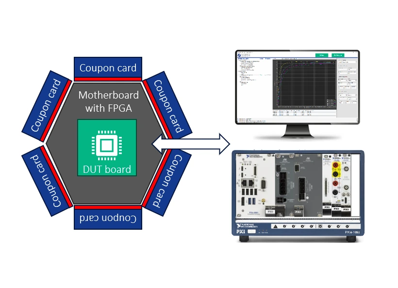
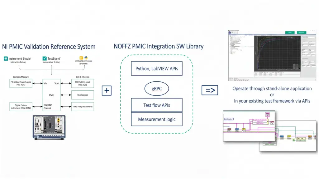
Validating Power Management ICs (PMICs) under real-world conditions is critical for ensuring overall system reliability — but building a custom validation setup from scratch can be time-consuming and resource-heavy. The NOFFZ + NI PMIC Validation System offers an off-the-shelf, modular solution that accelerates development while supporting seamless scaling for future test needs.
The system combines PXI-based hardware with an open-source software stack that includes pre-built measurement plug-ins for standard PMIC validation tasks like power sequencing, line/load regulation, efficiency, and load transients… With support for multiple IC variants, flexibility to customize, and easy automation, it’s built to reduce setup time and speed up your validation cycle.
Key Features
Precise rail sourcing and measurement with 40W SMUs
- ideal for characterizing voltage regulators and dynamic behavior
High-speed power testing with 300W supplies and e-loads with 1.8MS/s measurement
- capture fast load transients and ensure stable power delivery
Detailed signal visibility using 2–8 channel oscilloscopes (up to 1.5 Gbps BW)
- detect ripple, noise, and transient anomalies
Comprehensive protocol support, including I2C, I3C, SPI, SPMI – using NI Digital Pattern Instrument to verify communication under real operating conditions
- using NI Digital Pattern Instrument to verify communication under real operating conditions
Tightly synchronized instrumentation
- execute complex test scenarios with accurate timing alignment
WLR Test Framework
WLR TEST FRAMEWORK
WLR Test Framework
Parametric and wafer-level reliability testing place very specific demands on both instrumentation and software. Long-duration stress tests, tightly synchronized IV and CV measurements, complex sequencing, and strict requirements for reproducibility across wafers and test conditions are difficult to handle with generic test frameworks.
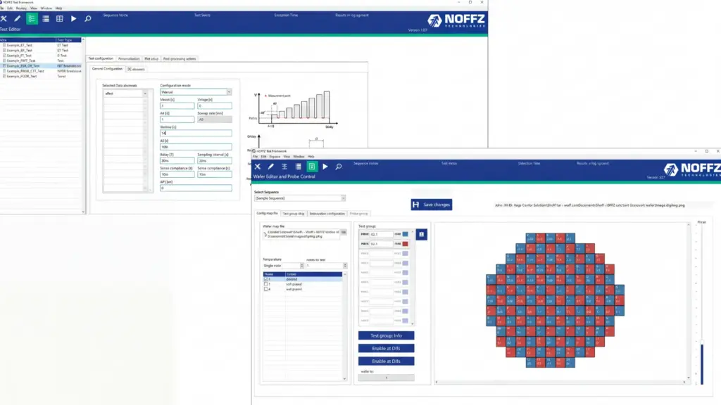
The NOFFZ WLR Test Framework is designed specifically for parametric and wafer-level reliability testing. The framework supports the complete parametric and WLR test flow, from detailed test parameterization and input sweeps to long-duration stress execution and result evaluation. Tests are built from preconfigured, reusable blocks and organized into sequences tailored to reliability campaigns. Integrated wafer mapping, prober automation, and temperature control enable efficient execution across selected dies, full wafers, or entire lots.
Key Capabilities
Comprehensive Parametric and WLR Test Coverage
- WLR Test Framework includes industry-standard parametric and reliability tests, such as IV, CV, TDDB, NBTI, CF, current collapse, RVS breakdown, and related stress measurements.
Support for Industry Standard Test Platforms
- The software runs natively on NI PXIe, NI STS, and Keysight B1500, enabling consistent parametric and reliability testing independent of the underlying hardware.
Sequencing Optimized for Long and Complex Tests
- Dedicated test and sequence editors allow precise control of stress profiles, timing, and measurement points without custom coding.
Integrated Prober and Wafer-Level Automation
- Built-in wafer map handling and prober control enable automated execution across selected dies, wafers, or lots, while still supporting manual control for engineering debug.
Unified Environment for Test, Execution, and Results
- A centralized user interface covering test definition, execution monitoring, live result visualization, post-processing, and reporting.
Digital Audio Data Test Instrument
Digital Audio Data Test Instrument
Digital Audio Data Test Instrument
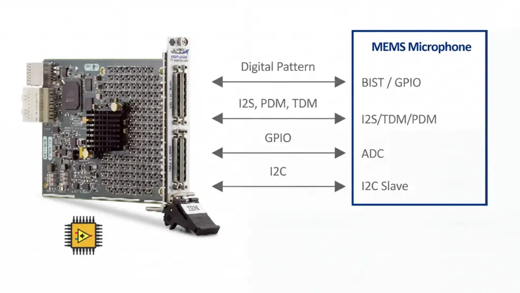
Modern MEMS microphones and audio ICs rely on digital audio protocols like I²S, PDM, and TDM. Testing these interfaces typically requires multiple tools — an FPGA-based protocol generator and analyzer, a Digital Pattern Instrument for custom signaling, and an I²C master to control the DUT. The NOFFZ Digital Audio Data Test Instrument combines all three into a single PXIe module, dramatically simplifying test setup and reducing system cost and complexity.
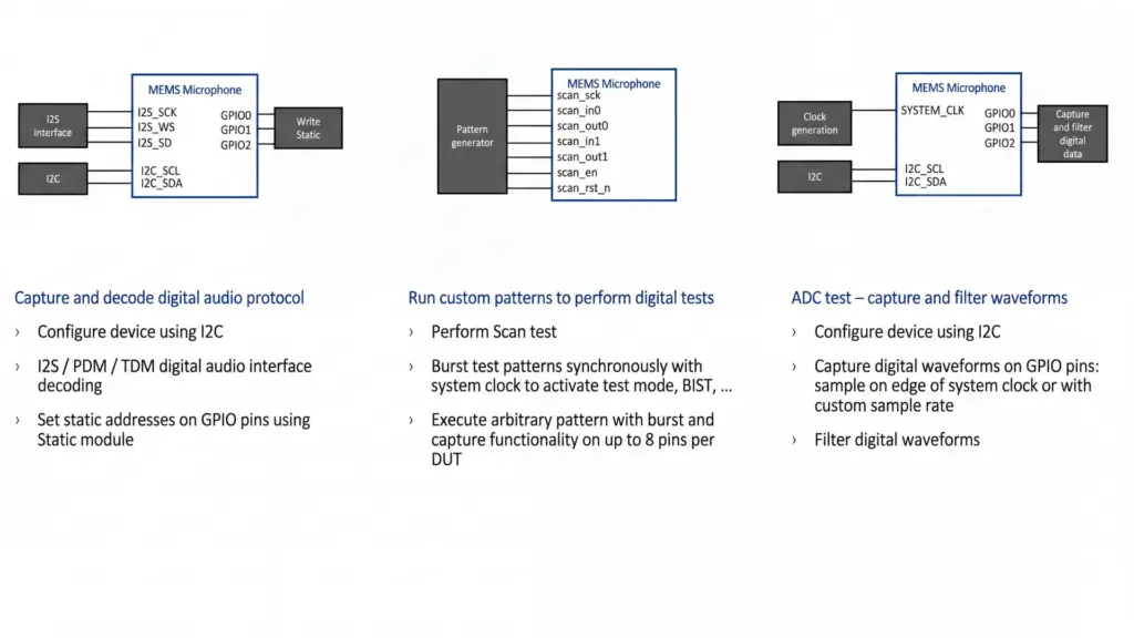
Built on FPGA and PXI technologies, the instrument offers a flexible and unified platform for testing audio interfaces across a variety of use cases. You can capture and decode digital audio protocols, run custom patterns to perform digital tests, or test your ADC by capturing and filtering waveforms — all from a single instrument.
What makes this solution effective
FPGA-based signal decoding and filtering
- Achieve ultra-fast test execution and efficient data handling
Digital pattern execution (.digipat)
- Run scan tests, enter test modes, burst signature patterns and more
Support for standard audio clock rates – 1.536 MHz, 3.072 MHz, 6.144 MHz, 12.288 MHz, with customizable options
- 1.536 MHz, 3.072 MHz, 6.144 MHz, 12.288 MHz, with customizable options
Triggering support – Easily synchronize with other PXI instruments in your bench
- Easily synchronize with other PXI instruments in your bench
High parallelism
- 128 DIO lines per PXIe slot, supporting up to 16 DUTs in parallel
Flexible software integration
- C#- und LabVIEW-APIs zum Erstellen kundenspezifischer Sequenzen oder zur Nutzung des NI TestStand Semiconductor Module
Need additional functionality? Our team can extend the instrument’s capabilities by modifying the FPGA code to support project-specific features, protocols, or timing requirements — tailored to your unique validation needs.
DO YOU HAVE ANY QUESTIONS?
Speak with our experts directly!
Let us know the details of your project. We’re curious about your ideas, products, and requirements and would be glad to advise you specifically about your requests.
Together we’ll make your project a success!
Let’s set up a meeting.